Table of Contents
I2C – Inter Integrated Circuit (Inter IC), also pronounced as “I squared C”
According to wiki, “I²C is a multi-master, multi-slave single-ended serial computer bus.
Simply it’s a one-to-many connection with in-band addressing in the messages.
INTRODUCTION
In brief, I2C is a synchronous protocol and it is the one which has some “intellect” in it while other protocols dumbly shifted bits in and out.
- I2C uses only 2 wires for signal, one for the clock (SCL) and one for the data (SDA), 3 if include ground & 4 if you also include power but they are available on PCB so don’t really count and allows to connect (ideally) 128 devices (practically approx. 112 devices, while other address reserves for some other purposes). This saves a ton of PCB wiring
- That means, master and slave send data over the same wire, controlled by the master who creates the clock signal
- I2C doesn’t use separate Slave Selects to select a particular device, but has addresses to identify slave device

I2C WORKING CONCEPT
1. IDLE STATE
Idle state of Lines SDA and SCL
-
- SDA: HIGH
- SCL: HIGH (square pulse)
2. Pull-up resistors
The I2C bus is wired with two pull-up resistors which pull the bus to a HIGH level, and the devices only send low levels. If devices want to send a High logic level they simply release the bus.
3. START and STOP signals
Master device controls the clock and generates the START and STOP signals. Slaves simply listen to the bus and act on data & clock that were sent by the master.
The master can send data to a slave or receive data from a slave while slaves do not transfer data between themselves.
START and STOP Bits defined as falling or rising edges on the data line while the clock line is kept high. Means to “Start” set SDA line from HIGH → LOW (falling edge) and to “Stop” set SDA line from LOW → HIGH (rising edge)

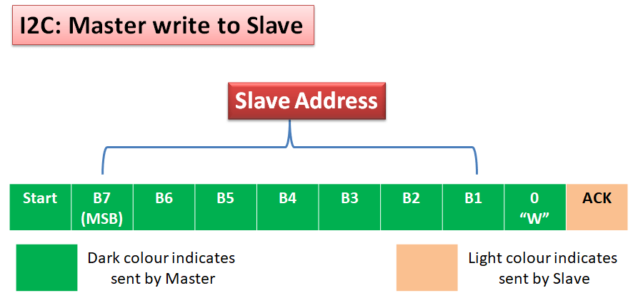
4. FIRST BYTE
The first byte (8-bit format) sent by the master, MSB first, holds a 7-bit address and a read/write bit which signifies whether the transaction will read/write to the slave, it indicates whether the next Byte(s) will come from the slave or master.
A LOW (0 or W) in read/write bit specifies that the master will write data to the addressed slave device.
A HIGH (1 or R) in read/write bit specifies that the master will read data from the addressed slave device.

5. ACKNOWLEDGEMENT
Receiver must send a “0” to acknowledge the reception of the Byte, after each Byte transfer.
6. I2C – MASTER WANTS TO WRITE
If the master device wants to write a byte, the same steps repeats
-
- Master transmit 1st Byte which contains a 7-bit slave address and write bit ‘0’, then an acknowledge bit transmitted by slave that it understands the address.
- After getting an acknowledgement bit, master transmits 2nd Byte which contains the register address (Data) where data to store, and again an acknowledge bit sent by slave.
- Then send 3rd Byte (Data) which contains data and receives an acknowledgement bit by the slave.

Master device any time can begin a transmission by pulling SDA low while SCL is high (a unique specific condition that other I2C devices identify as the start of a master transmission).
The slave device waits for the next 8 serial bits to see if it matches its individual address (each I2C must have a built-in unique address).
If it does recognise the next 7 bits as an address from the master device, the next ‘W’ as R/W bit tells the slave to read data coming from the master for the following packet (master writes). This sequence followed by the ACK bit that the slave must generate to indicate that it understood the address.
The diagram further down in the data transfer sequence shows this
When salve wants to generate the acknowledge bit (ACK signal), the master device releases the SDA line and the open-drain output is pulled high (idle state). This allows the slave device to generate the acknowledge bit (ACK signal) by pulling SDA low (only for that specific bit period).

DATA TRANSFER SEQUENCE IN I2C
Data transfer sequence from master to slave is, Master sends → S, ADDRESS, W, and then waits for the Slave signal which is an acknowledge bit (ACK) that will be generated by slave only, if the address sent by the master matches the slave’s internal address.
If this happens then the master sends DATA and waits for acknowledgement (ACK) from the slave. The master terminates the Byte transfer by generating a stop bit (P) (or repeat Start).
Note: One more protocol which uses the open – drain concept is the Dallas 1-wire protocol – but that is far slower. The benefit of the 1-wire protocol is that it permits powering and operating of the device through the one wire! It also allows communication (signal transmission) over very large distances unlike the I2C protocol.
7. I2C – MASTER WANTS TO READ DATA
Master only generates the clock pulses, If master wants to receive Data

When a master reads from the slave (data transfer from slave to master) in this case, instead of W, ‘R’ is sent as R/W bit. After data transmission from slave to the master, the master sends the acknowledge bit (ACK).
If the master does not want any more data it must send a not-acknowledge (NACK) which indicates to the slave that it should release the bus. This lets the master to send repeated START signal or the STOP bit (P).
Note: You must have two pull-up resistors for signal wires SCL and SDA
To save licensing costs this communication protocol was patented by NXP Semiconductors (formerly Phillips).
Word TWI (2-wire interface) which is exactly the same as I2C is used by ATMEL, it means any AVR device has TWI not I2C. You will often find devices that you realise are I2C compatible but they are labelled as using a ‘2 wire interface’. By not using the words ‘I2C’ manufacturers are avoiding paying royalties.
PROS – Advantages
- You can use 112 devices (ideally 128) on the bus
- Only two wires required.
CONS – Disadvantages
- The protocol designed for single board communication & too short not a long distance communication system between ICs on a single/same PCB
- You must have one pull-up resistor per signal wire (SCL & SDA).
SPEED
DATA RATE COMPARISON
I2C: The data rate has to be chosen between these
- 100 kbps – standard mode
- 400 kbps – fast mode
- 4 Mbps – high speed mode
But some I²C variants comprise
- 10 kbps – low speed mode
- 1 Mbps – fast mode
I2C is a serial protocol that can operate at different speeds 100 KHz, 400 KHz, and 3.4 MHz Not all chips support all speeds but 100 KHz is commonly supported.
COMPARING
I2C allows to have multiple master devices making programming the system more flexible. SPI is faster than I2C but in SPI there is no concept of multiple master devices.
CAN: Average of 2.5 Mbps
MORE DETAIL ON I2C
START (S) and STOP (P) bits
Only bus master can generate START (S) and STOP (P) bits a unique signals combination.
START bit reception by an I2C slave device resets its internal bus logic. This can be done at any time, so if anything goes wrong even in the middle of communication you can force a restart.
START and STOP bits are defined as falling or rising edge on the data line while the clock line is kept high.
DATA
All data blocks are composed of 8 bits. The first block has 7 address bits & a direction bit (Read or Write). Following blocks have 8 data bits. Acknowledge bits are squeezed in between each data block (a Bit after each Byte).
Each and every data Byte which is transmitted, has sequence as MSB first, including the address Byte.
To generate START, STOP or any data signal/bit, the data line (SDA) is used. It can only be done, when the clock is low, it must not change while the clock (SCL) is high.
ROBUST ACK SIGNALLING
I2C protocol has an acknowledgement feature which is not present in SPI. Due to this acknowledge system by the receiver, the sender knows whether data is accepted by the receiver or not. So we can say I2C is much better in a noisy environment.
Either the master or slave generates the acknowledge data bit, depending upon the direction of data transmission. For the master writing to a slave (W), acknowledge bit is generated by the slave, while master receiving (R) data from a slave, master generates the acknowledge bit.
Now there are 3 terms Acknowledge, No Acknowledge and Not Acknowledge (NACK)
Acknowledge ACK
The acknowledge bit generated by the receiver which indicates to the transmitter that the data received successfully. Only the master can create clock pulses for the acknowledge bit (or any bit).
Data transfer from master to slave
In this case the slave generates the acknowledge signal (SDA LOW)
What if no-acknowledge is received by the master? This means transfer has failed due to some issue. Then the master should generate a STOP or START again to abort the sequence.
No Acknowledge: Can only occur after a master has written a byte to a slave, means salve will generate an acknowledge bit.
No Acknowledge Condition
Actually this is not a condition. It is just a state in data flow between slave and master.
After transmission of the 8th bit from the master device to the slave device, the slave device doesn’t pull the SDA line LOW to acknowledge (in this case SDA is HIGH), then this condition is known as No-ACK condition.
Possible chances of No-ACK are as follows:
- The slave device is not there (no device on the address)
- The slave device missed a clock pulse and got out of sync with the SCL line generated by the master.
- The I2C bus is “stuck”.
In any of the above cases the master should abort the sequence by sending STOP condition on the bus.
Data transfer from slave to master
In this case the master generates the acknowledge signal (SDA LOW)
Generally, master generates an acknowledge bit (ACK) after it has received data. But if no more data is required on the last byte transfer, the master must generate a ‘not–acknowledge’ (NACK) instead of ACK bit. This makes the slave device stop sending data. Then the master generates the STOP bit or START again.
Not Acknowledge (NACK): Can only occur after a master has read a byte from a slave, means master will generate acknowledge bit.
Not Acknowledge (NACK):
If data sent from slave to master, master will generate ACK bit, after that, slave regains the control over SDA line, this could lead to problems.0
Now suppose, the next bit 0 is transmitting from slave to master, SDA line would be pulled LOW by slave (when SCL is LOW, only condition in which transaction happens). At the same time master wants to STOP transmission, master first releases SCL line (HIGH) and then try to release SDA line (HIGH), the condition to STOP, but SDA line is held under slave control then how master will release SDA line.
Result: Stop condition has not been generated on the bus and this condition is called as Not Acknowledge (NACK). Keep in mind No-ACK and Not-ACK is different.
Typical SDA and SCL signals transaction

Note: R/W (0 = write, 1 = read). ACK = 0 (pulled low by slave).
- Data transfer sequence
A general sequence of data transfer between Master and slave for I2C follows the following order:
- Master: Send the START bit (S)
- Master: Send the slave address (ADDR)
- Master: Send the Read(R) – 1 / Write (W) – 0 bit
- Salve: Send an acknowledge bit (ACK)
- DATA byte (8 bits) will be Send / Receive
- If W was sent by master: Master sends DATA
- If R was sent by master: Slave sends DATA
- Expect acknowledge bit (ACK)
- If W was sent by master: Salve sends ACK
- If R was sent by master: Master sends ACK
- Master: Send the STOP bit (P).
The steps 5 and 6 can be repeated so that a multiple Byte block can be read / written.
General call in I2C
The general call address is a reserved address, which is used by master to address all slave devices at once. Its address is 0000000 (7 bits) & written by master as 0000000W. If a device doesn’t need data from the general call structure it doesn’t need to respond to it. In fact the master device does not know how many devices respond to the general call. The second Byte, often determines the purpose of the general call.
General call can only write data to slaves but can’t read. You cannot select a specific device with it, all slaves should receive a general call, or you have to encode device address in general call message body and decode it in the slave.
Reserved addresses in I2C
Ideally 128 I2C addresses can be connected using 7 bit for address however some addresses reserved for some other purposes. Thus, practically only 112 addresses can be used with the 7 bit address scheme. To get rid of this use the 10 bit addresses method.
The table shows reserved I2C addresses for special purposes
| 10 bit addresses (In Binary form, left digit is MSB) |
Purpose |
| 0000000 0 | General Call |
| 0000000 1 | Start Byte |
| 0000001 X | CBUS Addresses |
| 0000010 X | Reserved for Different Bus Formats |
| 0000011 X | Reserved for future purposes |
| 00001XX X | High-Speed Master Code |
| 11110XX X | 10-bit Slave Addressing |
| 11111XX X | Reserved for future purposes |
READ NEXT
CAN – CONTROLLER AREA NETWORK